
|
| Patch antenna array |
| |
| GEMS is used to simulate the patch antenna array with the network system. A probe between the patch feed and ground plane, and the excitation, lumped port, is located the gap between the probe and ground plane. GEMS is used to optimize the gap between the ground and substrate. |
| |
| The basic design procedure in the simulation: |
 | Draw the substrate first and then assign the dielectric material to it | | Import the patch array model and assign it to be PEC, or draw it in GEMS designer, | | Draw a probe that touches the feed point of the antenna feed network | | Draw a line between the probe and ground plane | | Define the line as a lumped port | | Define the optimized dimension as a parameter, and associate it to all the objects or options | | Specify the list of parameter values (GEMS will run for each case, and collect the simulation result for each case in one file) | | Specify the domain size and boundary. | | Generate the adaptive mesh | | Specify the convergence criterion | | Simulate the project using a single PC or cluster |
|
| The basic settings in the simulation: |
| Option | Setting | Description | | Boundary | PML truncates all six walls | Open space problem | | Excitation | Lumped port | Use a small gap between the probe and ground plane | | Mesh | Non-uniform | The mesh should pass the key edges of antenna structure | | Output | S-parameters, far field pattern | Outputs variation with the parametric dimension | | Simulation | A multiple core PC | |
|
| |
Patch Antenna Array | 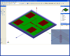 | | | 2-D Far Field Patterns | 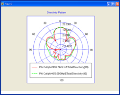 |
| Return Loss | 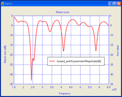 | | | Optimized S-parameter | 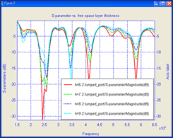 |
| 3-D Directivity Pattern | 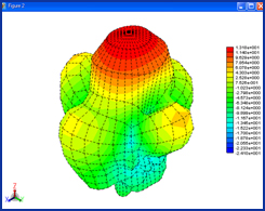 | | | 3-D Current Distribution (1) | 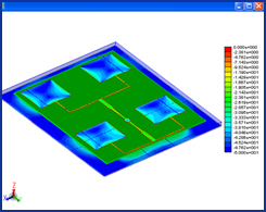 |
|
|
3-D Current Distribution (2) | 3-D Current Distribution (3) | 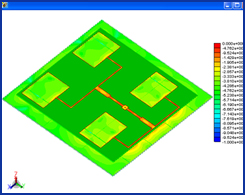 | 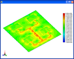 |
|