| ||||||||||||||||||
| High speed chip | ||||||||||||||||||
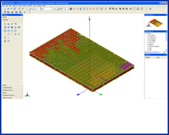
| The high speed chip model (including 8 layers) was provided by IBM. The chip dimensions are 15000 um x 15325 um x 772 um. The width and thickness of signal line are 25 um and 8 um, respectively. We can get excellent results using the cell sizes, Dx=12.5um and Dz=8um. No other time domain solver can simulate it. However, it is not a big problem for GEMS, since GEMS allows us to bring the absorbing boundary one or two cells from the chip structure. | ||||||||||||||||||
| ||||||||||||||||||
|